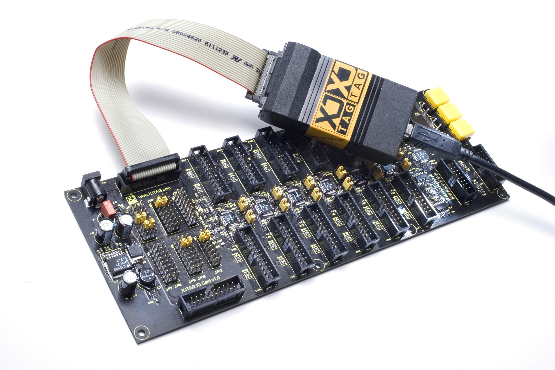
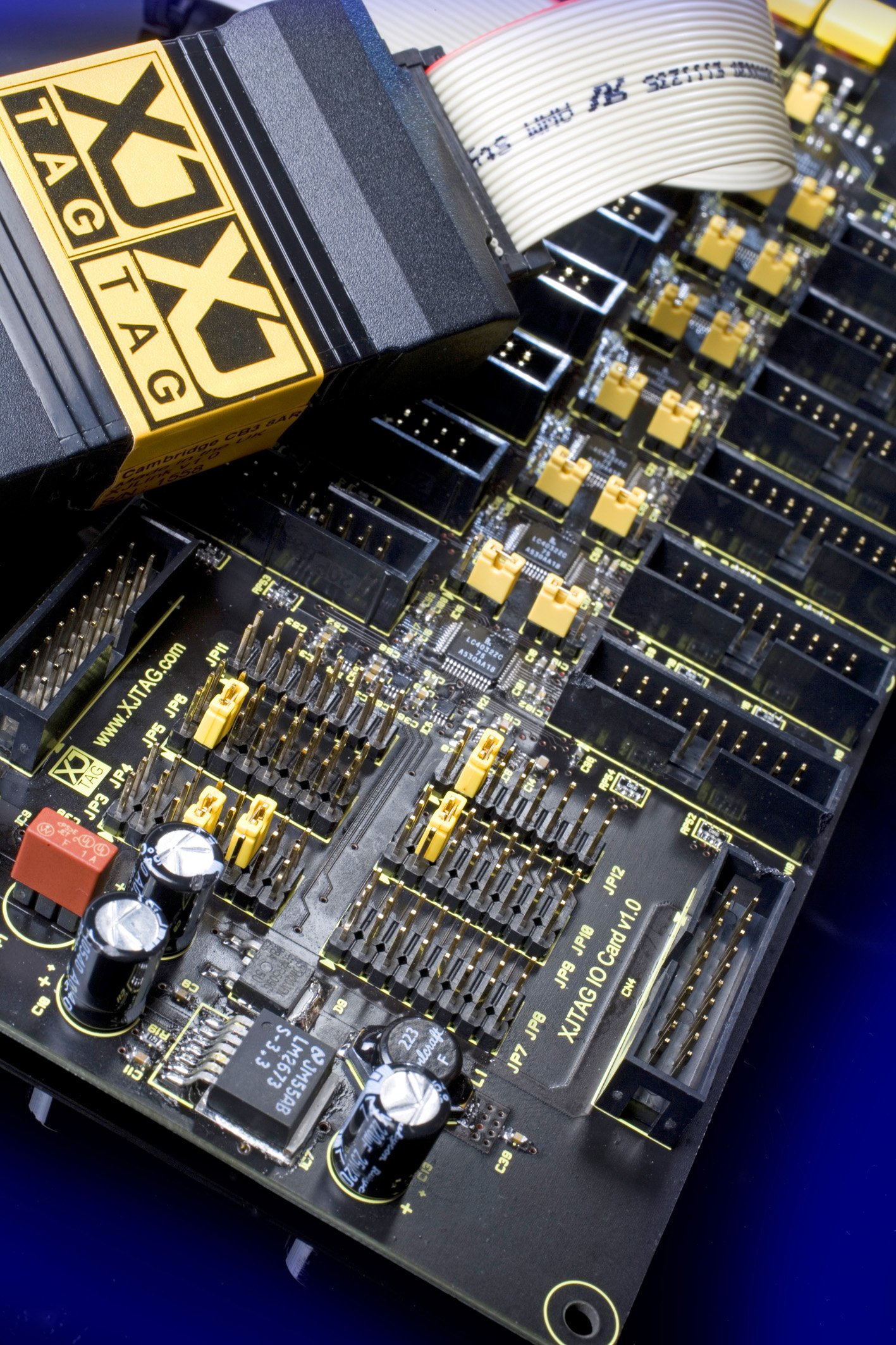
- The XJIO board reduces fault diagnosis times on failed circuits by up to 50% as it can eradicate the need for loopbacks, cable swapping and costly custom test jigs
- The XJIO board is designed predominantly for testing circuits with large amounts of digital I/O; the board features 208 digital I/Os and is expandable by daisy-chaining boards together
- The XJIO board provides ‘black box’ testing for non-JTAG boards; also features 16 analogue I/Os which facilitate a range of testing including power rail level verification
CAMBRIDGE, England, May 10, 2006 – XJTAG, a leading supplier of boundary scan development tools, today announced an enhancement to its award-winning XJTAG Development System. The new XJIO expansion board improves test coverage and fault diagnosis on complex printed circuits, checks power rail levels and can eliminate the need for costly custom test jigs.
The XJIO board improves the test coverage for a Unit Under Test (UUT) by verifying the signals right through to the external connections. In the event of a board failure, the fault diagnosis times can be reduced by as much as half, as the board eradicates the need for time-consuming loopbacks and cable swapping.
With 208 digital and 16 analogue (8xADCs and 8xDACs) I/Os, the XJIO board provides customers developing JTAG and non-JTAG boards with a cost-effective and reusable alternative to traditional test fixtures. Custom test jigs are costly and are increasingly difficult to justify given shortening product development times and the increasing frequency of board re-spins.
“The XJIO board was developed predominantly for testing circuits with large amounts of digital I/O such as on network cards – particularly if the board has more outputs than inputs or vice-versa,” said Dominic Plunkett, XJTAG’s chief technology officer. “It features over 200 digital I/Os and this density can be expanded to many thousands by daisy-chaining the XJIO boards together using the reconfigurable external JTAG connector.”
The XJIO board can be powered from USB, for quick and portable test setup. Alternatively, if more than 80mA of current is required, there is a connector for a standard 12V power supply. All the connectors on the XJIO board are standard IDC, for economical and efficient cable assemblies. Furthermore, the switches and LEDs enable additional test control, allowing customers to develop a complete and repeatable test solution.
“The XJIO board extends the advantages of JTAG testing to non-JTAG boards,” added Dominic Plunkett. “This facilitates a range of testing, including power rail level verification using the onboard ADCs, and provides a ‘black box’ solution for testing non-JTAG boards.”
Used in conjunction with the XJTAG Development System, the XJIO board enables circuit designers to cut the cost and shorten the development cycle of electronic products. The XJTAG system can test a high proportion of the circuit (both JTAG and non-JTAG devices) including BGA and chip scale devices, SDRAMs, Ethernet controllers, video interfaces, Flash memories, FPGAs (Field Programmable Gate Arrays), microprocessors and many other devices. XJTAG also enables In-System Programming of FPGAs, CPLDs (Complex Programmable Logic Devices) and Flash memories.
The XJTAG Development System meets the growing market need for a cost-effective solution for testing printed circuit boards populated with JTAG devices such as BGA and chip scale devices. Such devices cannot be effectively tested by traditional methods such as flying probes, logic analyzers, oscilloscopes and X-ray systems.
The XJTAG Development System incorporates XJAnalyser, XJEase, XJRunner, XJLink and XJDemo. XJAnalyser is a powerful tool for circuit visualisation that provides a simple graphical view of the state of all JTAG pins. XJEase is the high-level, C-like test description language for manipulating non-JTAG devices. XJRunner is a production optimised version of the XJTAG Development System, designed specifically for contract manufacturers and production sites.
XJLink is a USB 2.0 hardware module used to connect the computer with the unit under test. XJDemo is a fully populated demonstrator board, with tutorials designed to provide the developer with a rapid understanding of the XJTAG system and how to simulate faults.
For more information about the XJTAG Development System, please contact XJTAG, St John’s Innovation Centre, Cowley Road, Cambridge, CB4 0DS, UK. Telephone +44 (0) 1223 223007, fax +44 (0) 1223 223009 or email enquiries@xjtag.com. Alternatively visit old.xjtag.com.
About XJTAG (old.xjtag.com)
XJTAG is a specialist design and test tool developer. Its JTAG (Joint Test Action Group) development system offers a competitive solution for designers and developers of electronic circuits. Utilising XJTAG allows the circuit development and prototyping process to be shortened significantly by facilitating early test development, early design validation, fast development of functional tests and test re-use across circuits that use the same devices. The company is based in the UK at St John’s Innovation Centre, Cowley Road, Cambridge. XJTAG is part of the Cambridge Technology Group (www.cambridgetechgroup.com).
What is JTAG?
Advances in silicon design, such as increasing device density and, more recently, ball grid array (BGA) and chip scale packaging, have reduced the efficacy of traditional electronic circuit testing methods. In order to overcome these problems and others; some of the world’s leading silicon manufacturers combined to form the Joint Test Action Group (JTAG). The findings of this group were used as the basis for the Institute of Electrical and Electronic Engineers (IEEE) standard 1149.1: Standard Test Access Port and Boundary Scan Architecture and subsequently the standard became known as JTAG.
Images (Click for high resolution versions)
XJTAG XJIO board


