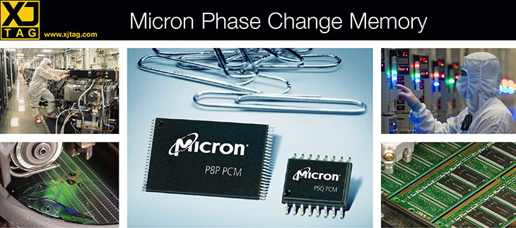
Micron Phase Change Memory is a groundbreaking new memory technology from global semiconductor innovator Micron Technology. When perfecting it, the development team partnered with XJTAG to create a solution suitable for programming in production or in the laboratory. XJTAG drew on XJFlash, its successful Flash-programming solution, to program PCM at the highest possible speed.
Micron Phase Change Memory (PCM) is an innovative new non-volatile technology capable of matching the best read and write performance of alternatives such as NAND/NOR Flash, DRAM, and EEPROM. It has low read latency, similar to NOR Flash, and matches the read bandwidth of DRAM. The write speed is comparable to that of NAND Flash, with the added advantage that no separate erase cycle is required.
“PCM is a compelling new memory technology that combines the best attributes found in NOR, NAND and DRAM,” says Jeff Bader, senior director of marketing for Micron’s embedded group.
To complete development, Micron PCM’s designers needed an effective solution enabling customers to program the new devices in a laboratory or at high speed on a production line. The nature of the technology called for in-system programming, because PCM chips are programmed after reflow soldering.
In-system programming is commonly used with Non-Volatile Memory (NVM) such as Flash, to boot-up and test boards during manufacture, program completed products, and apply software updates in the field. Most boundary scan test systems are able to perform in-system programming of Flash through the JTAG (IEEE 1149.1) connection.
Depending on the device types, JTAG chain length and TCK clock frequency, programming non-volatile memory using a JTAG connection can often take 60 µs or longer for a single write cycle. At this rate the programming time for a 128 Mbit Flash can be over eight minutes. Hence in-system programming via JTAG has traditionally been most effective only with very small data images.
The XJTAG boundary scan system, however, can program Flash much more quickly thanks to its unique XJFlash capability. XJFlash overcomes the bandwidth limitations of the JTAG serial interface and is able to program the chip at the practical maximum speed, provided there is an FPGA or CPU on the target board and this is connected to the JTAG chain correctly. For a comparable 128 Mbit device, XJFlash can reduce the total programming time to less than 20 seconds, with an average write-cycle time of under 2 µs.
Building on the IP contained within XJFlash, XJTAG engineers also achieved programming times better than 20 seconds for similar PCM chips. This is close to the typical programming time specified by Micron. “Because PCM is a new technology, it is imperative that we build a strong ecosystem of support to further customer adoption. We are pleased with the work XJTAG has done in building a programming solution, enabling PCM to be easily deployed in a production environment,” adds Jeff Bader.
With this enhancement to the XJTAG system now adding in-system programming for Micron PCM devices, with the shortest possible programming time, engineers designing complex boards containing BGA, FPGA and NVM devices can avoid using a separate programmer and use the XJTAG system to debug, test and program their designs throughout the product lifecycle.
A white paper explaining high speed programming of non-volatile memories is available from the XJTAG website at old.xjtag.com.


